The part number MC74HCT373ADTR2G corresponds to a specific integrated circuit (IC) manufactured by ON Semiconductor. The MC74HCT373ADTR2G is a high-speed CMOS octal D-type latch with 3-state outputs. It is a member of the HCT series, which is characterized by its compatibility with TTL logic levels.
Here are some details about the MC74HCT373ADTR2G:
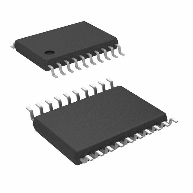
1.Package Type: The MC74HCT373ADTR2G is available in a 20-pin TSSOP (Thin Shrink Small Outline Package) package. TSSOP packages have a thin profile and small footprint, making them suitable for space-constrained applications.
2.Supply Voltage: The operating supply voltage range for the MC74HCT373ADTR2G is typically between 4.5V and 5.5V.
3.Logic Family: It belongs to the HCT (High-Speed CMOS TTL-Compatible) logic family. The HCT logic family provides compatibility with both CMOS and TTL logic levels, allowing for easy integration with existing TTL-based systems.
4.Number of Latches: The MC74HCT373ADTR2G consists of eight D-type latches, making it an octal latch.
5.3-State Outputs: Each latch in the MC74HCT373ADTR2G has a 3-state output, which allows the outputs to be enabled or disabled, providing flexibility in controlling the output signals.
6.Clock Input: The MC74HCT373ADTR2G features a clock (CLK) input that controls the latch operation. When the clock input is triggered, the data at the D inputs is latched and reflected at the corresponding Q outputs.
7.3-State Output Enable Input: It has an output enable (OE) input that enables or disables the 3-state outputs of the latch. When the OE input is high, the outputs are in the high-impedance state, allowing multiple devices to share a common bus.
8.Operating Temperature Range: The MC74HCT373ADTR2G is typically designed to operate within a temperature range of -40°C to +85°C.
Please note that the specific electrical characteristics, timing diagrams, pin configurations, and application guidelines can be found in the official datasheet provided by ON Semiconductor for the MC74HCT373ADTR2G.
The MC74HCT373ADTR2G is an octal D-type latch with 3-state outputs. Here are some characteristics of this product:
1.High-Speed Operation: The MC74HCT373ADTR2G is designed for high-speed operation, allowing for efficient data latching and transfer.
2.3-State Outputs: Each of the eight latches in the device has a 3-state output. This feature enables the outputs to be either actively driven or put into a high-impedance state.
3.Data Latching: The latch operation is controlled by a clock (CLK) input. When the clock signal transitions, the data at the input (D) pins is latched and reflected at the corresponding output (Q) pins.
4.Output Enable Function: The MC74HCT373ADTR2G includes an output enable (OE) input. When the OE input is high, the 3-state outputs are enabled and actively driven. When the OE input is low, the outputs are placed into a high-impedance state.
5.Compatibility: The MC74HCT373ADTR2G is compatible with both CMOS and TTL logic levels. This makes it suitable for interfacing with different logic families and systems.
6.Package Type: The MC74HCT373ADTR2G is available in a 20-pin TSSOP (Thin Shrink Small Outline Package) package. This package offers a compact size and is suitable for space-constrained applications.
These characteristics make the MC74HCT373ADTR2G well-suited for applications that require data storage and transfer, such as digital systems, memory circuits, and control interfaces. For detailed information on the electrical characteristics, timing diagrams, pin configurations, and application guidelines, it is recommended to refer to the official datasheet provided by the manufacturer.
Tags:MC74HCT373ADTR2G

