The CD4015BF is a specific part number associated with a CMOS dual 4-bit static shift register. Here are some details regarding the CD4015BF:
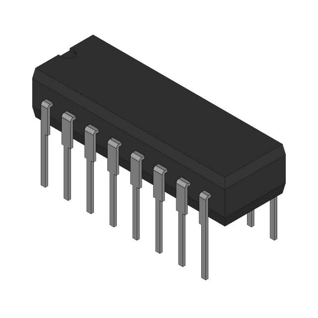
1.Package Type: The CD4015BF is typically available in a 16-pin DIP (Dual In-Line Package) format.
2.Supply Voltage: It operates with a supply voltage range of 3V to 18V.
3.Logic Family: The CD4015BF belongs to the CMOS (Complementary Metal-Oxide-Semiconductor) logic family.
4.Logic Function: It is a dual 4-bit static shift register, meaning it can store and shift 4 bits of data.
5.Clock Inputs: The CD4015BF has two clock inputs: Clock (CLK) and Reset (RESET). The CLK input is used to shift the data, while the RESET input is used to clear or reset the shift register.
6.Serial Data Input: It has a serial data input (SER) for inputting data into the shift register.
7.Parallel Data Outputs: The CD4015BF provides two sets of 4 parallel data outputs (Q0-Q3 and Q0'-Q3'), corresponding to the two sections of the shift register.
8.Operating Temperature Range: The operating temperature range for the CD4015BF is typically -55°C to +125°C.
Please note that while these details provide a general overview of the CD4015BF, it's essential to consult the official datasheet provided by the manufacturer for precise and detailed information. The datasheet will contain comprehensive information about the electrical characteristics, timing diagrams, pin configurations, and application guidelines specific to the CD4015BF.
The CD4015BF is a CMOS dual 4-bit static shift register. As for the characteristics of this specific part, here are some key features typically associated with the CD4015BF:
1.High-Speed Operation: The CD4015BF is designed for high-speed operation, allowing for efficient data shifting and processing.
2.Versatile Shift Register: It provides a dual 4-bit shift register configuration, allowing for parallel loading and serial shifting of data.
3.Serial Data Input: The CD4015BF has a single serial data input (SER) that enables the input of data into the shift register.
4.Parallel Data Outputs: It offers two sets of 4 parallel data outputs (Q0-Q3 and Q0'-Q3') corresponding to the two sections of the shift register. These outputs provide access to the stored data.
5.Clock and Reset Inputs: The CD4015BF features clock (CLK) and reset (RESET) inputs. The CLK input controls the shifting of data, while the RESET input allows for clearing or resetting the shift register.
6.Wide Supply Voltage Range: It typically operates within a supply voltage range of 3V to 18V, making it compatible with various voltage levels.
7.Low Power Consumption: The CD4015BF is designed to consume low power, making it suitable for power-sensitive applications.
8.Operating Temperature Range: The CD4015BF is typically designed to operate within a temperature range of -55°C to +125°C, allowing for use in various environmental conditions.
It's important to refer to the official datasheet provided by the manufacturer for precise and detailed information about the characteristics, electrical specifications, timing diagrams, pin configurations, and application guidelines of the CD4015BF. The datasheet will provide comprehensive information specific to this part number.
Tags:CD4015BF