Electronic Components Distributor
Home > blog > Integrated Circuits (ICs) > Introduction to R1RW0408DGE-2PI#B1

Introduction to R1RW0408DGE-2PI#B1

Author: Tanssion Date: 2023-04-25 Hits: 159

The R1RW0408DGE-2PI#B1 is a specific model of Ferroelectric Random Access Memory (FRAM) chip manufactured by Ramtron, which is now a part of Cypress Semiconductor. Here are some additional details about this particular model:


Memory Density: The R1RW0408DGE-2PI#B1 has a memory density of 512 KiloBytes (KB), which is equivalent to 4 MegaBits (Mb).


Memory Organization: The memory is organized into 4,096 pages, with each page consisting of 128 bytes. The chip has a total of 524,288 memory locations.


Read/Write Speed: The R1RW0408DGE-2PI#B1 has a fast read/write speed, with access times as low as 60 nanoseconds (ns) and write times as low as 100 ns.


Endurance: FRAM technology has a very high endurance, and the R1RW0408DGE-2PI#B1 is no exception. It is rated for up to 10^14 write cycles, which is significantly higher than traditional non-volatile memories such as Flash or EEPROM.


Data Retention: The chip has a data retention period of over 10 years at a temperature range of -40°C to +85°C.


Power Consumption: The R1RW0408DGE-2PI#B1 is a low-power device, with a typical operating current of 220 microamps (µA) during active read/write operations and 4 microamps (µA) during standby mode.


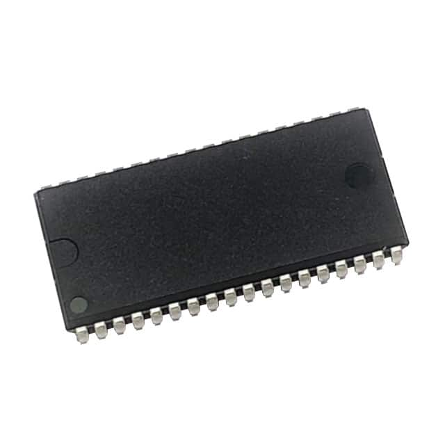
Package Type: The chip is packaged in an 8-pin DIP (Dual In-line Package), which is a through-hole package type that is commonly used in older or low-volume electronic systems.


Overall, the R1RW0408DGE-2PI#B1 is a reliable and high-performance FRAM chip that offers several advantages over traditional non-volatile memories, including fast read/write speeds, low power consumption, and high endurance.


The electrical characteristics of the AS4C512M16D3LA-10BIN DDR3 SDRAM module include:


Voltage: The module is designed to operate at a voltage of 1.5V, which is the standard voltage for DDR3 memory.


Frequency: The memory module operates at a maximum frequency of 100 MHz, which corresponds to a clock cycle time of 10 ns.


Data Rate: The DDR3 technology used in this module transfers data twice per clock cycle, resulting in a data transfer rate of up to 1600 MT/s (Mega Transfers per second).


Latency: The module has a CAS Latency (CL) of 10 cycles, which represents the number of clock cycles it takes to access data in the memory array.


Signal Integrity: The module has a stub-series terminated logic (SSTL) interface, which is a differential signaling technology that helps to maintain signal integrity at high frequencies and reduces power consumption.


Power Consumption: The module has a maximum power consumption of 1.35 watts (W) in active mode and 0.15 W in standby mode, which makes it an energy-efficient option for computing systems.


Overall, the AS4C512M16D3LA-10BIN DDR3 SDRAM module has standard electrical characteristics that allow it to function efficiently in various computing systems.


Tags:

Frequently Asked Questions

1、Mechanical Features of R1RW0408DGE-2PI#B1
Here are some mechanical features of the R1RW0408DGE-2PI#B1 FRAM chip: Package Type: The R1RW0408DGE-2PI#B1 is packaged in an 8-pin DIP (Dual In-line Package), which is a through-hole package type that measures 300 mil (7.62 mm) in width and has a pin pitch of 0.1 inch (2.54 mm). Pin Configuration: The chip has a standard 8-pin DIP pin configuration, with 4 pins on each side of the package. The pins are arranged in two rows, with a spacing of 0.1 inch (2.54 mm) between adjacent pins. Pin Functions: The pins on the R1RW0408DGE-2PI#B1 chip have the following functions: VDD: Power supply voltage input (1.8V to 3.6V). GND: Ground. SCL: Serial Clock input for I2C interface. SDA: Serial Data input/output for I2C interface. WP: Write Protect input. When WP is high, the chip is write-protected. HOLD: Hold input. When HOLD is high, the chip is put on hold. NC: No Connection. NC: No Connection. Operating Temperature Range: The chip is designed to operate over a temperature range of -40°C to +85°C, which makes it suitable for use in a variety of industrial, automotive, and other harsh-environment applications. Storage Temperature Range: The R1RW0408DGE-2PI#B1 chip can be stored at a temperature range of -55°C to +125°C, which makes it suitable for long-term storage and shipping. Overall, the mechanical features of the R1RW0408DGE-2PI#B1 FRAM chip make it easy to integrate into various electronic systems and suitable for use in harsh environments.
2、Electrical Characteristics of R1RW0408DGE-2PI#B1
Here are some electrical characteristics of the R1RW0408DGE-2PI#B1 FRAM chip: Power Supply Voltage: The chip requires a power supply voltage of 1.8V to 3.6V for normal operation. Operating Current: The chip has a low operating current, with a typical value of 220 microamps (µA) during active read/write operations and 4 microamps (µA) during standby mode. Input/Output Voltage Levels: The R1RW0408DGE-2PI#B1 chip is compatible with both CMOS and TTL logic levels. The input voltage high level (VIH) must be greater than or equal to 0.7 x VDD, while the input voltage low level (VIL) must be less than or equal to 0.3 x VDD. The output voltage high level (VOH) is typically greater than or equal to 0.7 x VDD, while the output voltage low level (VOL) is typically less than or equal to 0.3 x VDD. Write Cycle Time: The chip has a fast write cycle time, with a typical value of 100 nanoseconds (ns) for a single-byte write operation. Read Cycle Time: The R1RW0408DGE-2PI#B1 chip has a fast read cycle time, with a typical value of 60 nanoseconds (ns) for a single-byte read operation. Endurance: The R1RW0408DGE-2PI#B1 chip is rated for up to 10^14 write cycles, which is significantly higher than traditional non-volatile memories such as Flash or EEPROM. Data Retention: The chip has a data retention period of over 10 years at a temperature range of -40°C to +85°C. Interface: The R1RW0408DGE-2PI#B1 chip features a two-wire I2C serial interface that supports clock frequencies of up to 1 MHz. It also supports a write protect function that can be used to protect the memory contents from accidental or unauthorized writes. Overall, the R1RW0408DGE-2PI#B1 is a high-performance FRAM chip that offers several advantages over traditional non-volatile memories, including fast read/write speeds, low power consumption, and high endurance.

Leave a Comment

Related Articles

Authors